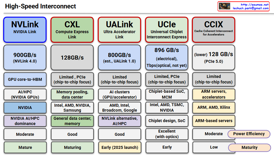
Deepseek v3 Large-Scale Network Architecture Analysis
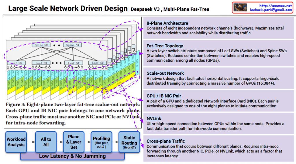
This image explains the Multi-Plane Fat-Tree network structure of Deepseek v3.
Core Architecture
1. 8-Plane Architecture
- Consists of eight independent network channels (highways)
- Maximizes network bandwidth and distributes traffic for enhanced scalability
2. Fat-Tree Topology
- Two-layer switch structure:
- Leaf SW (Leaf Switches): Directly connected to GPUs
- Spine SW (Spine Switches): Interconnect leaf switches
- Enables high-speed communication among all nodes (GPUs) while minimizing switch contention
3. GPU/IB NIC Pair
- Each GPU is paired with a dedicated Network Interface Card (NIC)
- Each pair is exclusively assigned to one of the eight planes to initiate communication
Communication Methods
NVLink
- Ultra-high-speed connection between GPUs within the same node
- Fast data transfer path used for intra-node communication
Cross-plane Traffic
- Occurs when communication happens between different planes
- Requires intra-node forwarding through another NIC, PCIe, or NVLink
- Primary factor that increases latency
Network Optimization Process
The workflow below minimizes latency and prevents network congestion:
- Workload Analysis
- All to All (analyzing all-to-all communication patterns)
- Plane & Layer Set (plane and layer assignment)
- Profiling (Hot-path opt K) (hot-path optimization)
- Static Routing (Hybrid) (hybrid static routing approach)
Goal: Low latency & no jamming
Scalability
This design is a scale-out network for large-scale distributed training supporting 16,384+ GPUs. Each plane operates independently to maximize overall system throughput.
3-Line Summary
Deepseek v3 uses an 8-plane fat-tree network architecture that connects 16,384+ GPUs through independent communication channels, minimizing contention and maximizing bandwidth. The two-layer switch topology (Spine and Leaf) combined with dedicated GPU-NIC pairs enables efficient traffic distribution across planes. Cross-plane traffic management and hot-path optimization ensure low-latency, high-throughput communication for large-scale AI training.
#DeepseekV3 #FatTreeNetwork #MultiPlane #NetworkArchitecture #ScaleOut #DistributedTraining #AIInfrastructure #GPUCluster #HighPerformanceComputing #NVLink #DataCenterNetworking #LargeScaleAI
With Claude