Chiplet

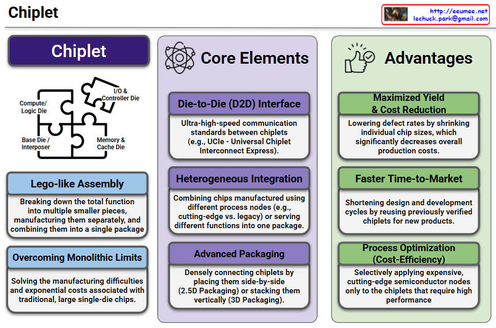
This infographic provides a highly structured and clear overview of Chiplet technology, dividing the subject into its core concept, essential technological elements, and primary business advantages.

1. The Concept of a Chiplet (Left Section)

  • Visual Metaphor: The jigsaw puzzle perfectly illustrates the architecture of a chiplet-based system. It shows distinct functional dies—Compute/Logic Die, I/O & Controller Die, and Memory & Cache Die—fitting together onto a Base Die / Interposer to form a complete processor.
  • Lego-like Assembly: Instead of manufacturing one massive chip, the total processing function is broken down into smaller, specialized pieces (chiplets). These are manufactured separately and then assembled into a single unified package.
  • Overcoming Monolithic Limits: This modular approach directly solves the physical manufacturing challenges and the exponential costs associated with traditional, large single-die (monolithic) semiconductors.

2. Core Elements (Middle Section)

This section highlights the three foundational technologies required to make chiplets function seamlessly:

  • Die-to-Die (D2D) Interface: This refers to the ultra-high-speed communication standards (such as the UCIe – Universal Chiplet Interconnect Express) that allow the physically separated chiplets to exchange data with minimal latency, acting as one cohesive unit.
  • Heterogeneous Integration: This is the technological capability to combine chips manufactured using entirely different process nodes (e.g., pairing a cutting-edge 3nm compute node with a mature 14nm I/O node) or serving completely different functions into one single package.
  • Advanced Packaging: The intricate physical process of densely connecting these chiplets, whether by placing them side-by-side on a silicon interposer (2.5D Packaging) or stacking them vertically like a skyscraper (3D Packaging).

3. Advantages (Right Section)

The rightmost column outlines the strategic and financial benefits of adopting the chiplet architecture:

  • Maximized Yield & Cost Reduction: Smaller chiplets are statistically much less prone to manufacturing defects than large monolithic chips. Shrinking the individual die size lowers defect rates, maximizes wafer yield, and drastically reduces overall production costs.
  • Faster Time-to-Market: Semiconductor companies can reuse existing, pre-verified chiplet designs (like “off-the-shelf” I/O or memory controllers) for new products. This significantly shortens the design, research, and development cycles.
  • Process Optimization (Cost-Efficiency): It allows for extreme cost-efficiency by reserving the most expensive, cutting-edge semiconductor nodes exclusively for the chiplets that demand the highest performance (like the main logic), while using cheaper, legacy nodes for less demanding components.

📌 Summary

Chiplet technology represents a critical paradigm shift in semiconductor manufacturing. By transitioning from monolithic designs to a modular, “lego-like” assembly—enabled by advanced packaging, heterogeneous integration, and high-speed D2D interfaces—the industry can overcome physical scaling limits. This architecture not only slashes manufacturing costs and improves yield but also accelerates innovation, making it the foundational technology driving today’s high-performance AI accelerators and advanced data center operations.

#Chiplet #Semiconductor #AdvancedPackaging #HeterogeneousIntegration #UCIe #AIChips #HighPerformanceComputing #HPC #TechInfographic #TechInnovation

With Gemini

Next AI Computing


The Evolution of AI Computing

The provided images illustrate the architectural shift in AI computing from the traditional “Separation” model to a “Unified” brain-inspired model, focusing on overcoming energy inefficiency and data bottlenecks.

1. CURRENT: The Von Neumann Wall (Separation)

  • Status: The industry standard today.
  • Structure: Computation (CPU/GPU) and Memory (DRAM) are physically separate.
  • Problem: Constant data movement between components creates a “Von Neumann Wall” (bottleneck).
  • Efficiency: Extremely wasteful; 60-80% of energy is consumed just moving data, not processing it.

2. BRIDGE: Processing-In-Memory (PIM) (Proximity)

  • Status: Practical, near-term solution; nearly commercial-ready.
  • Structure: Small processing units are embedded inside the memory.
  • Benefit: Processes data locally to provide a 2-10x efficiency boost.
  • Primary Use: Ideal for accelerating Large Language Models (LLMs).

3. FUTURE: Neuromorphic Computing (Unity)

  • Status: Future-oriented paradigm shift.
  • Structure: Compute IS memory, mimicking the human brain’s architecture where memory elements perform calculations.
  • Benefit: Eliminates data travel entirely, promising a massive 1,000x+ energy improvement.
  • Requirement: Requires a complete overhaul of current software stacks.
  • Primary Use: Ultra-low power Edge devices and Robotics.

#AIComputing #NextGenAI #VonNeumannWall #PIM #ProcessingInMemory #NeuromorphicComputing #EnergyEfficiency #LLM #EdgeAI #Semiconductor #FutureTech #ComputerArchitecture

With Gemini

SRAM, DRAM, HBM

The image provides a comprehensive comparison of SRAM, DRAM, and HBM, which are the three pillars of modern memory architecture. For an expert in AI infrastructure, this hierarchy explains why certain hardware choices are made to balance performance and cost.


1. SRAM (Static Random Access Memory)

  • Role: Ultra-Fast Cache. It serves as the immediate storage for the CPU/GPU to prevent processing delays.
  • Location: On-die. It is integrated directly into the silicon of the processor chip.
  • Capacity: Very small (MB range) due to the large physical size of its 6-transistor structure.
  • Cost: Extremely Expensive (~570x vs. DRAM). This is the “prime real estate” of the semiconductor world.
  • Key Insight: Its primary goal is Latency-focus. It ensures the most frequently used data is available in nanoseconds.

2. DRAM (Dynamic Random Access Memory)

  • Role: Main System Memory. It is the standard “workspace” for a server or PC.
  • Location: Motherboard Slots (DIMM). It sits externally to the processor.
  • Capacity: Large (GB to TB range). It is designed to hold the OS and active applications.
  • Cost: Relatively Affordable (1x). It serves as the baseline for memory pricing.
  • Key Insight: It requires a constant “Refresh” to maintain data, making it “Dynamic,” but it offers the best balance of capacity and price.

3. HBM (High Bandwidth Memory)

  • Role: AI Accelerators & Supercomputing. It is the specialized engine behind modern AI GPUs like the NVIDIA H100.
  • Location: In-package. It is stacked vertically (3D Stack) and placed right next to the GPU die on a silicon interposer.
  • Capacity: High (Latest versions offer 141GB+ per stack).
  • Cost: Very Expensive (Premium, ~6x vs. DRAM).
  • Key Insight: Its primary goal is Throughput-focus. By widening the data “highway,” it allows the GPU to process massive datasets (like LLM parameters) without being bottlenecked by memory speed.

📊 Technical Comparison Summary

FeatureSRAMDRAMHBM
Speed TypeLow LatencyModerateHigh Bandwidth
Price Factor570x1x (Base)6x
PackagingIntegrated in ChipExternal DIMM3D Stacked next to Chip

💡 Summary

  1. SRAM offers ultimate speed at an extreme price, used exclusively for tiny, critical caches inside the processor.
  2. DRAM is the cost-effective “standard” workspace used for general system tasks and large-scale data storage.
  3. HBM is the high-bandwidth solution for AI, stacking memory vertically to feed data-hungry GPUs at lightning speeds.

#SRAM #DRAM #HBM3e #AIInfrastructure #GPUArchitecture #Semiconductor #DataCenter #HighBandwidthMemory #TechComparison

with Gemini

AI Workload with Power/Cooling


Breakdown of the “AI Workload with Power/Cooling” Diagram

This diagram illustrates the flow of Power and Cooling changes throughout the execution stages of an AI workload. It divides the process into five phases, explaining how data center infrastructure (Power, Cooling) reacts and responds from the start to the completion of an AI job.

Here are the key details for each phase:

1. Pre-Run (Preparation Phase)

  • Work Job: Job Scheduling.
  • Key Metric: Requested TDP (Thermal Design Power). It identifies beforehand how much heat the job is expected to generate.
  • Power/Cooling: PreCooling. This is a proactive measure where cooling levels are increased based on the predicted TDP before the job actually starts and heat is generated.

2. Init / Ramp-up (Initialization Phase)

  • Work Job: Context Loading. The process of loading AI models and data into memory.
  • Key Metric: HBM Power Usage. The power consumption of High Bandwidth Memory becomes a key indicator.
  • Power/Cooling: As VRAM operates, Power consumption begins to rise (Power UP).

3. Execution (Execution Phase)

  • Work Job: Kernel Launch. The point where actual computation kernels begin running on the GPU.
  • Key Metric: Power Draw. The actual amount of electrical power being drawn.
  • Power/Cooling: Instant Power Peak. A critical moment where power consumption spikes rapidly as computation begins in earnest. The stability of the power supply unit (PSU) is vital here.

4. Sustained (Heavy Load Phase)

  • Work Job: Heavy Load. Continuous heavy computation is in progress.
  • Key Metric: Thermal/Power Cap. Monitoring against set limits for temperature or power.
  • Power/Cooling:
    • Throttling: If “What-if” scenarios occur (such as power supply leaks or reaching a Thermal Over-Limit), protection mechanisms activate. DVFS (Dynamic Voltage and Frequency Scaling) triggers Throttling (Down Clock) to protect the hardware.

5. Cooldown (Completion Phase)

  • Work Job: Job Complete.
  • Key Metric: Power State. The state changes to “Change Down.”
  • Power/Cooling: Although the job is finished, Residual Heat remains in the hardware. Instead of shutting off fans immediately, Ramp-down Control is used to cool the equipment gradually and safely.

Summary & Key Takeaways

This diagram demonstrates that managing AI infrastructure goes beyond simply “running a job.” It requires active control of the infrastructure (e.g., PreCooling, Throttling, Ramp-down) to handle the specific characteristics of AI workloads, such as rapid power spikes and high heat generation.

Phase 1 (PreCooling) for proactive heat management and Phase 4 (Throttling) for hardware protection are the core mechanisms determining the stability and efficiency of an AI Data Center.


#AI #ArtificialIntelligence #GPU #HPC #DataCenter #AIInfrastructure #DataCenterOps #GreenIT #SustainableTech #SmartCooling #PowerEfficiency #PowerManagement #ThermalEngineering #TDP #DVFS #Semiconductor #SystemArchitecture #ITOperations

With Gemini