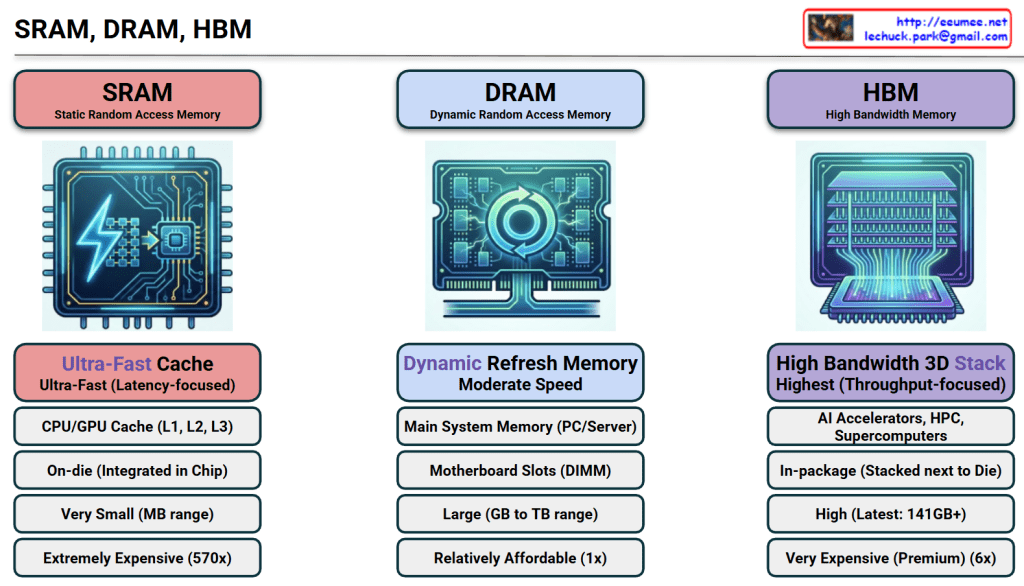
The image provides a comprehensive comparison of SRAM, DRAM, and HBM, which are the three pillars of modern memory architecture. For an expert in AI infrastructure, this hierarchy explains why certain hardware choices are made to balance performance and cost.
1. SRAM (Static Random Access Memory)
- Role: Ultra-Fast Cache. It serves as the immediate storage for the CPU/GPU to prevent processing delays.
- Location: On-die. It is integrated directly into the silicon of the processor chip.
- Capacity: Very small (MB range) due to the large physical size of its 6-transistor structure.
- Cost: Extremely Expensive (~570x vs. DRAM). This is the “prime real estate” of the semiconductor world.
- Key Insight: Its primary goal is Latency-focus. It ensures the most frequently used data is available in nanoseconds.
2. DRAM (Dynamic Random Access Memory)
- Role: Main System Memory. It is the standard “workspace” for a server or PC.
- Location: Motherboard Slots (DIMM). It sits externally to the processor.
- Capacity: Large (GB to TB range). It is designed to hold the OS and active applications.
- Cost: Relatively Affordable (1x). It serves as the baseline for memory pricing.
- Key Insight: It requires a constant “Refresh” to maintain data, making it “Dynamic,” but it offers the best balance of capacity and price.
3. HBM (High Bandwidth Memory)
- Role: AI Accelerators & Supercomputing. It is the specialized engine behind modern AI GPUs like the NVIDIA H100.
- Location: In-package. It is stacked vertically (3D Stack) and placed right next to the GPU die on a silicon interposer.
- Capacity: High (Latest versions offer 141GB+ per stack).
- Cost: Very Expensive (Premium, ~6x vs. DRAM).
- Key Insight: Its primary goal is Throughput-focus. By widening the data “highway,” it allows the GPU to process massive datasets (like LLM parameters) without being bottlenecked by memory speed.
📊 Technical Comparison Summary
| Feature | SRAM | DRAM | HBM |
| Speed Type | Low Latency | Moderate | High Bandwidth |
| Price Factor | 570x | 1x (Base) | 6x |
| Packaging | Integrated in Chip | External DIMM | 3D Stacked next to Chip |
💡 Summary
- SRAM offers ultimate speed at an extreme price, used exclusively for tiny, critical caches inside the processor.
- DRAM is the cost-effective “standard” workspace used for general system tasks and large-scale data storage.
- HBM is the high-bandwidth solution for AI, stacking memory vertically to feed data-hungry GPUs at lightning speeds.
#SRAM #DRAM #HBM3e #AIInfrastructure #GPUArchitecture #Semiconductor #DataCenter #HighBandwidthMemory #TechComparison
with Gemini

