Linux kernel for GPU Workload

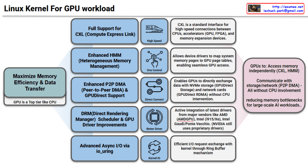
Linux Kernel GPU Workload Support Features

Goal: Maximize Memory Efficiency & Data Transfer

The core objective is to treat GPUs as a top-tier component like CPUs, reducing memory bottlenecks for large-scale AI workloads.

Key Features

1. Full CXL (Compute Express Link) Support

  • Standard interface for high-speed connections between CPUs, accelerators (GPU, FPGA), and memory expansion devices
  • Enables high-speed data transfer

2. Enhanced HMM (Heterogeneous Memory Management)

  • Heterogeneous memory management capabilities
  • Allows device drivers to map system memory pages to GPU page tables
  • Enables seamless GPU memory access

3. Enhanced P2P DMA & GPUDirect Support

  • Enables direct data exchange between GPUs
  • Direct communication with NVMe storage and network cards (GPUDirect RDMA)
  • Operates without CPU intervention for improved performance

4. DRM Scheduler & GPU Driver Improvements

  • Enhanced Direct Rendering Manager scheduling functionality
  • Active integration of latest drivers from major vendors: AMD (AMDGPU), Intel (i915/Xe), Intel Gaudi/Ponte Vecchio
  • NVIDIA still uses proprietary drivers

5. Advanced Async I/O via io_uring

  • Efficient I/O request exchange with kernel through Ring Buffer mechanism
  • Optimized asynchronous I/O performance

Summary

The Linux kernel now enables GPUs to independently access memory (CXL, HMM), storage, and network resources (P2P DMA, GPUDirect) without CPU involvement. Enhanced drivers from AMD, Intel, and improved schedulers optimize GPU workload management. These features collectively eliminate CPU bottlenecks, making the kernel highly efficient for large-scale AI and HPC workloads.

#LinuxKernel #GPU #AI #HPC #CXL #HMM #GPUDirect #P2PDMA #AMDGPU #IntelGPU #MachineLearning #HighPerformanceComputing #DRM #io_uring #HeterogeneousComputing #DataCenter #CloudComputing

With Claude

CXL ( Compute express link )

Traditional CPU-GPU vs CXL Key Comparison

🔴 PCIe System Inefficiencies

Separated Memory Architecture

  • Isolated Memory: CPU(DDR4) ↔ GPU(VRAM) completely separated
  • Mandatory Data Copying: CPU Memory → PCIe → GPU Memory → Computation → Result Copy
  • PCIe Bandwidth Bottleneck: Limited to 64GB/s maximum

Major Overheads

  • Memory Copy Latency: Tens of ms to seconds for large data transfers
  • Synchronization Wait: CPU cache flush + GPU synchronization
  • Memory Duplication: Same data stored in both CPU and GPU memory

🟢 CXL Core Improvements

1. Unified Memory Architecture

Before: CPU [Memory] ←PCIe→ [Memory] GPU (Separated)
After: CPU ←CXL→ GPU → Shared Memory Pool (Unified)

2. Zero-Copy & Hardware Cache Coherency

  • Eliminates Memory Copying: Data access through pointer sharing only
  • Automatic Synchronization: CXL controller ensures cache coherency at HW level
  • Real-time Sharing: GPU can immediately access CPU-modified data

3. Performance Improvements

MetricPCIe 4.0CXL 2.0Improvement
Bandwidth64 GB/s128 GB/s2x
Latency1-2μs200-400ns5-10x
Memory CopyRequiredEliminatedComplete Removal

🚀 Practical Benefits

AI/ML: 90% reduction in training data loading time, larger model processing capability
HPC: Real-time large dataset exchange, memory constraint elimination
Cloud: Maximized server resource efficiency through memory pooling


💡 CXL Core Innovations

  1. Zero-Copy Sharing – Eliminates physical data movement
  2. HW-based Coherency – Complete removal of software synchronization overhead
  3. Memory Virtualization – Scalable memory pool beyond physical constraints
  4. Heterogeneous Optimization – Seamless integration of CPU, GPU, FPGA, etc.

The key technical improvements of CXL – Zero-Copy sharing and hardware-based cache coherency – are emphasized as the most revolutionary aspects that fundamentally solve the traditional PCIe bottlenecks.

With Claude

CPU with GPU (legacy)

This image is a diagram explaining the data transfer process between CPU and GPU. Let me interpret the main components and processes.

Key Components

Hardware:

  • CPU: Main processor
  • GPU: Graphics processing unit (acting as accelerator)
  • DRAM: Main memory on CPU side
  • VRAM: Dedicated memory on GPU side
  • PCIe: High-speed interface connecting CPU and GPU

Software/Interfaces:

  • Software (Driver/Kernel): Driver/kernel controlling hardware
  • DMA (Direct Memory Access): Direct memory access

Data Transfer Process (4 Steps)

Step 1 – Data Preparation

  • CPU first writes data to main memory (DRAM)

Step 2 – DMA Transfer

  • Copy data from main memory to GPU’s VRAM via PCIe
  • ⚠️ Wait Time: Cache Flush – CPU cache is flushed before accelerator can access the data

Step 3 – Task Execution

  • GPU performs tasks using the copied data

Step 4 – Result Copy

  • After task completion, GPU copies results back to main memory
  • ⚠️ Wait Time: Synchronization – CPU must perform another synchronization operation before it can read the results

Performance Considerations

This diagram shows the major bottlenecks in CPU-GPU data transfer:

  • Memory copy overhead: Data must be copied twice (CPU→GPU, GPU→CPU)
  • Synchronization wait times: Synchronization required at each step
  • PCIe bandwidth limitations: Physical constraints on data transfer speed

CXL-based Improvement Approach

CXL (Compute Express Link) shown on the right side of the diagram represents next-generation technology for improving this data transfer process, offering an alternative approach to solve the complex 4-step process and related performance bottlenecks.


Summary

This diagram demonstrates how CPU-GPU data transfer involves a complex 4-step process with performance bottlenecks caused by memory copying overhead, synchronization wait times, and PCIe bandwidth limitations. CXL is presented as a next-generation technology solution that can overcome the limitations of traditional data transfer methods.

With Claude

High-Speed Interconnect

This image compares five major high-speed interconnect technologies:

NVLink (NVIDIA Link)

  • Speed: 900GB/s (NVLink 4.0)
  • Use Case: GPU core-to-HBM, AI/HPC with NVIDIA GPUs
  • Features: NVIDIA proprietary, dominates AI/HPC market
  • Maturity: Mature

CXL (Compute Express Link)

  • Speed: 128GB/s
  • Use Case: Memory pooling, data center, general data center memory
  • Features: Supported by Intel, AMD, NVIDIA, Samsung; PCIe-based with chip-to-chip focus
  • Maturity: Maturing

UALink (Ultra Accelerator Link)

  • Speed: 800GB/s (estimated, UALink 1.0)
  • Use Case: AI clusters, GPU/accelerator interconnect
  • Features: Led by AMD, Intel, Broadcom, Google; NVLink alternative
  • Maturity: Early (2025 launch)

UCIe (Universal Chiplet Interconnect Express)

  • Speed: 896GB/s (electrical), 7Tbps (optical, not yet available)
  • Use Case: Chiplet-based SoC, MCM (Multi-Chip Module)
  • Features: Supported by Intel, AMD, TSMC, NVIDIA; chiplet design focus
  • Maturity: Early stage, excellent performance with optical version

CCIX (Cache Coherent Interconnect for Accelerators)

  • Speed: 128GB/s (PCIe 5.0-based)
  • Use Case: ARM servers, accelerators
  • Features: Supported by ARM, AMD, Xilinx; ARM-based server focus
  • Maturity: Low, limited power efficiency

Summary: All technologies are converging toward higher bandwidth, lower latency, and chip-to-chip connectivity to address the growing demands of AI/HPC workloads. The effectiveness varies by ecosystem, with specialized solutions like NVLink leading in performance while universal standards like CXL focus on broader compatibility and adoption.

With Claude