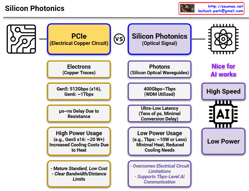
This diagram compares PCIe (Electrical Copper Circuit) and Silicon Photonics (Optical Signal) technologies.
PCIe (Left, Yellow Boxes)
- Signal Transmission: Uses electrons (copper traces)
- Speed: Gen5 512Gbps (x16), Gen6 ~1Tbps expected
- Latency: μs~ns level delay due to resistance
- Power Consumption: High (e.g., Gen5 x16 ~20W), increased cooling costs due to heat generation
- Pros/Cons: Mature standard with low cost, but clear bandwidth/distance limitations
Silicon Photonics (Right, Purple Boxes)
- Signal Transmission: Uses photons (silicon optical waveguides)
- Speed: 400Gbps~7Tbps (utilizing WDM technology)
- Latency: Ultra-low latency (tens of ps, minimal conversion delay)
- Power Consumption: Low (e.g., 7Tbps ~10W or less), minimal heat with reduced cooling needs
- Key Benefits:
- Overcomes electrical circuit limitations
- Supports 7Tbps-level AI communication
- Optimized for AI workloads (high speed, low power)
Key Message
Silicon Photonics overcomes the limitations of existing PCIe technology (high power consumption, heat generation, speed limitations), making it a next-generation technology particularly well-suited for AI workloads requiring high-speed data processing.
With Claude
