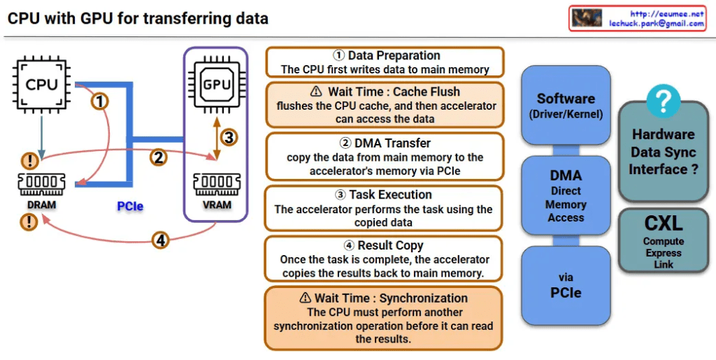
This image is a diagram explaining the data transfer process between CPU and GPU. Let me interpret the main components and processes.
Key Components
Hardware:
- CPU: Main processor
- GPU: Graphics processing unit (acting as accelerator)
- DRAM: Main memory on CPU side
- VRAM: Dedicated memory on GPU side
- PCIe: High-speed interface connecting CPU and GPU
Software/Interfaces:
- Software (Driver/Kernel): Driver/kernel controlling hardware
- DMA (Direct Memory Access): Direct memory access
Data Transfer Process (4 Steps)
Step 1 – Data Preparation
- CPU first writes data to main memory (DRAM)
Step 2 – DMA Transfer
- Copy data from main memory to GPU’s VRAM via PCIe
- ⚠️ Wait Time: Cache Flush – CPU cache is flushed before accelerator can access the data
Step 3 – Task Execution
- GPU performs tasks using the copied data
Step 4 – Result Copy
- After task completion, GPU copies results back to main memory
- ⚠️ Wait Time: Synchronization – CPU must perform another synchronization operation before it can read the results
Performance Considerations
This diagram shows the major bottlenecks in CPU-GPU data transfer:
- Memory copy overhead: Data must be copied twice (CPU→GPU, GPU→CPU)
- Synchronization wait times: Synchronization required at each step
- PCIe bandwidth limitations: Physical constraints on data transfer speed
CXL-based Improvement Approach
CXL (Compute Express Link) shown on the right side of the diagram represents next-generation technology for improving this data transfer process, offering an alternative approach to solve the complex 4-step process and related performance bottlenecks.
Summary
This diagram demonstrates how CPU-GPU data transfer involves a complex 4-step process with performance bottlenecks caused by memory copying overhead, synchronization wait times, and PCIe bandwidth limitations. CXL is presented as a next-generation technology solution that can overcome the limitations of traditional data transfer methods.
With Claude


