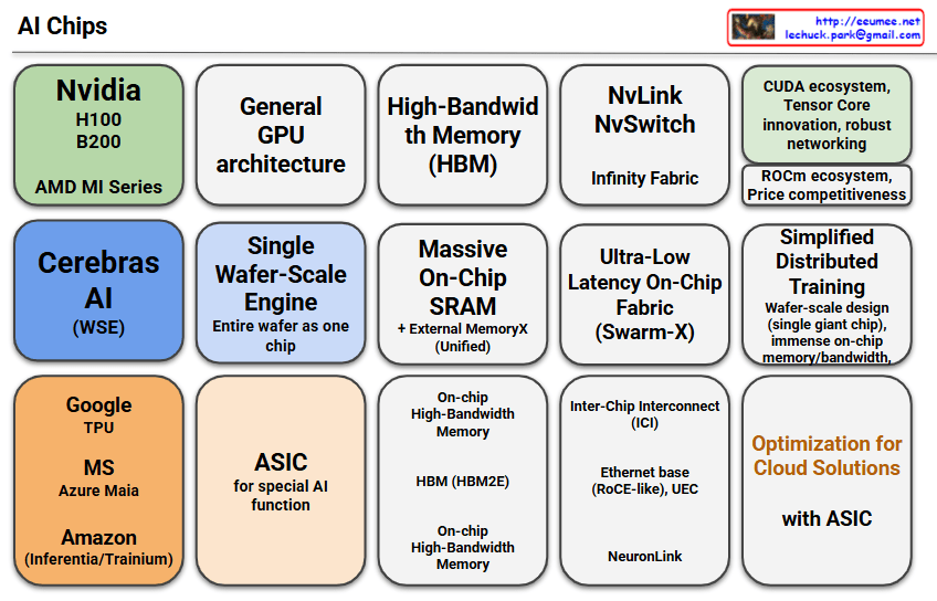
This image presents a comprehensive overview of the AI chip ecosystem, categorizing different approaches and technologies:
Major AI Chip Categories
GPU-Based Solutions:
- Nvidia H100/B200 (AMD MI Series): Currently the most widely used GPUs for AI training and inference
- General GPU architecture: Traditional general-purpose GPU architectures
Specialized AI Chips:
- Cerebras AI (WSE): Wafer-Scale Engine where the entire wafer functions as one chip
- Google TPU: Google’s Tensor Processing Unit
- MS Azure Maia: Microsoft’s cloud-optimized AI chip
- Amazon (Inferentia/Trainium): Amazon’s dedicated inference and training chips
Technical Features
Memory Technologies:
- High-Bandwidth Memory (HBM): Advanced memory technology including HBM2E
- Massive On-Chip SRAM: Large-capacity on-chip memory with external MemoryX
- Ultra-Low Latency On-Chip Fabric (SwarmX): High-speed on-chip interconnect
Networking Technologies:
- NvLink/NvSwitch: Nvidia’s high-speed interconnect with Infinity Fabric
- Inter-Chip Interconnect (ICI): Ethernet-based connections including RoCE-like and UEC protocols
- NeuroLink: Advanced chip-to-chip communication
Design Approaches:
- Single Wafer-Scale Engine: Entire wafer as one chip with immense on-chip memory/bandwidth
- Simplified Distributed Training: Wafer-scale design enabling simplified distributed training
- ASIC for special AI function: Application-specific integrated circuits optimized for AI workloads
- Optimization for Cloud Solutions with ASIC: Cloud-optimized ASIC implementations
This diagram effectively illustrates the evolution from general-purpose GPUs to specialized AI chips, showcasing how different companies are pursuing distinct technological approaches to meet the demanding requirements of AI workloads. The ecosystem demonstrates various strategies including memory optimization, interconnect technologies, and architectural innovations.
With Claude
