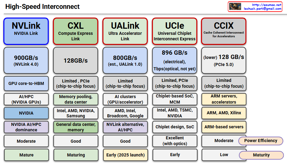
This image compares five major high-speed interconnect technologies:
NVLink (NVIDIA Link)
- Speed: 900GB/s (NVLink 4.0)
- Use Case: GPU core-to-HBM, AI/HPC with NVIDIA GPUs
- Features: NVIDIA proprietary, dominates AI/HPC market
- Maturity: Mature
CXL (Compute Express Link)
- Speed: 128GB/s
- Use Case: Memory pooling, data center, general data center memory
- Features: Supported by Intel, AMD, NVIDIA, Samsung; PCIe-based with chip-to-chip focus
- Maturity: Maturing
UALink (Ultra Accelerator Link)
- Speed: 800GB/s (estimated, UALink 1.0)
- Use Case: AI clusters, GPU/accelerator interconnect
- Features: Led by AMD, Intel, Broadcom, Google; NVLink alternative
- Maturity: Early (2025 launch)
UCIe (Universal Chiplet Interconnect Express)
- Speed: 896GB/s (electrical), 7Tbps (optical, not yet available)
- Use Case: Chiplet-based SoC, MCM (Multi-Chip Module)
- Features: Supported by Intel, AMD, TSMC, NVIDIA; chiplet design focus
- Maturity: Early stage, excellent performance with optical version
CCIX (Cache Coherent Interconnect for Accelerators)
- Speed: 128GB/s (PCIe 5.0-based)
- Use Case: ARM servers, accelerators
- Features: Supported by ARM, AMD, Xilinx; ARM-based server focus
- Maturity: Low, limited power efficiency
Summary: All technologies are converging toward higher bandwidth, lower latency, and chip-to-chip connectivity to address the growing demands of AI/HPC workloads. The effectiveness varies by ecosystem, with specialized solutions like NVLink leading in performance while universal standards like CXL focus on broader compatibility and adoption.
With Claude
